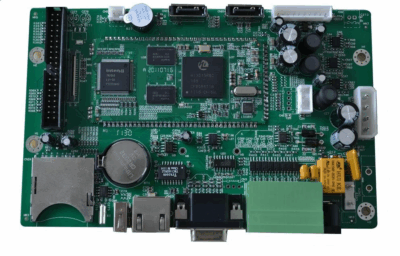
Medical PCBA manufacturing is part of Electronic Manufacturing Services (EMS), which focuses on providing circuit board assembly services for medical devices such as monitoring equipment, diagnostic equipment, and imaging equipment.
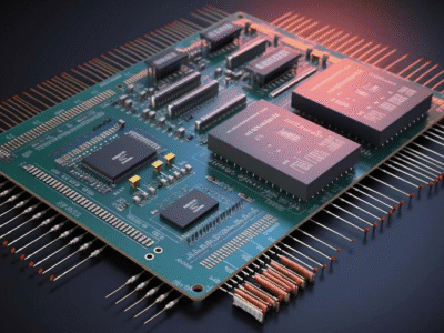
Medical PCB Manufacturing
- Design Imaging: Use a plotter to convert design files into films (like photo negatives). For inner layers, black ink represents copper circuits and clear ink non-conductive areas; the outer layer uses the opposite ink logic.
- Inner Layer Copper Printing: Laminate copper layers onto both sides of a fiberglass substrate. After UV curing, chemical development, and etching, desired copper circuits remain. Multilayer boards repeat this step before lamination.
- Layer Combination: After inner layer etching, printing, and lamination, drill holes to connect layers. High-precision medical PCBs use optical/laser drilling with alignment pins for accuracy.
- Outer Layer Imaging: Apply photoresist to outer copper layers in a clean area. Clean the copper surface, align black ink transparencies with pins, cure photoresist with UV light, and remove unhardened resist covered by black ink.
- Outer Layer Etching: Remove excess outer copper, add copper via electroplating, and use electroplated tin to protect critical areas. Post-etching, AOI inspection ensures compliance, even for complex circuits.
- Surface Finishing: Apply a conductive coating to the finished PCB as per customer requirements.
Application of Medical PCBA
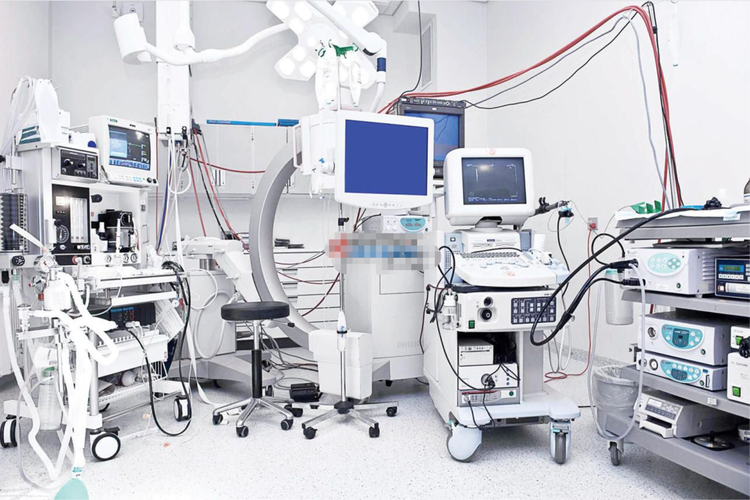
- Diagnostic Equipment: X-ray devices, MRI, ultrasonic testing equipment, etc.
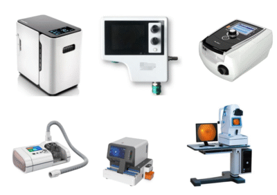
- Therapeutic Equipment: radiotherapy equipment, electrical stimulation devices.
- Patient Monitoring: ECG monitors, blood oxygen saturation monitors.
- Personal Health Management: blood glucose testers, blood pressure monitors and other wearable devices.
Medical PCBA Processing
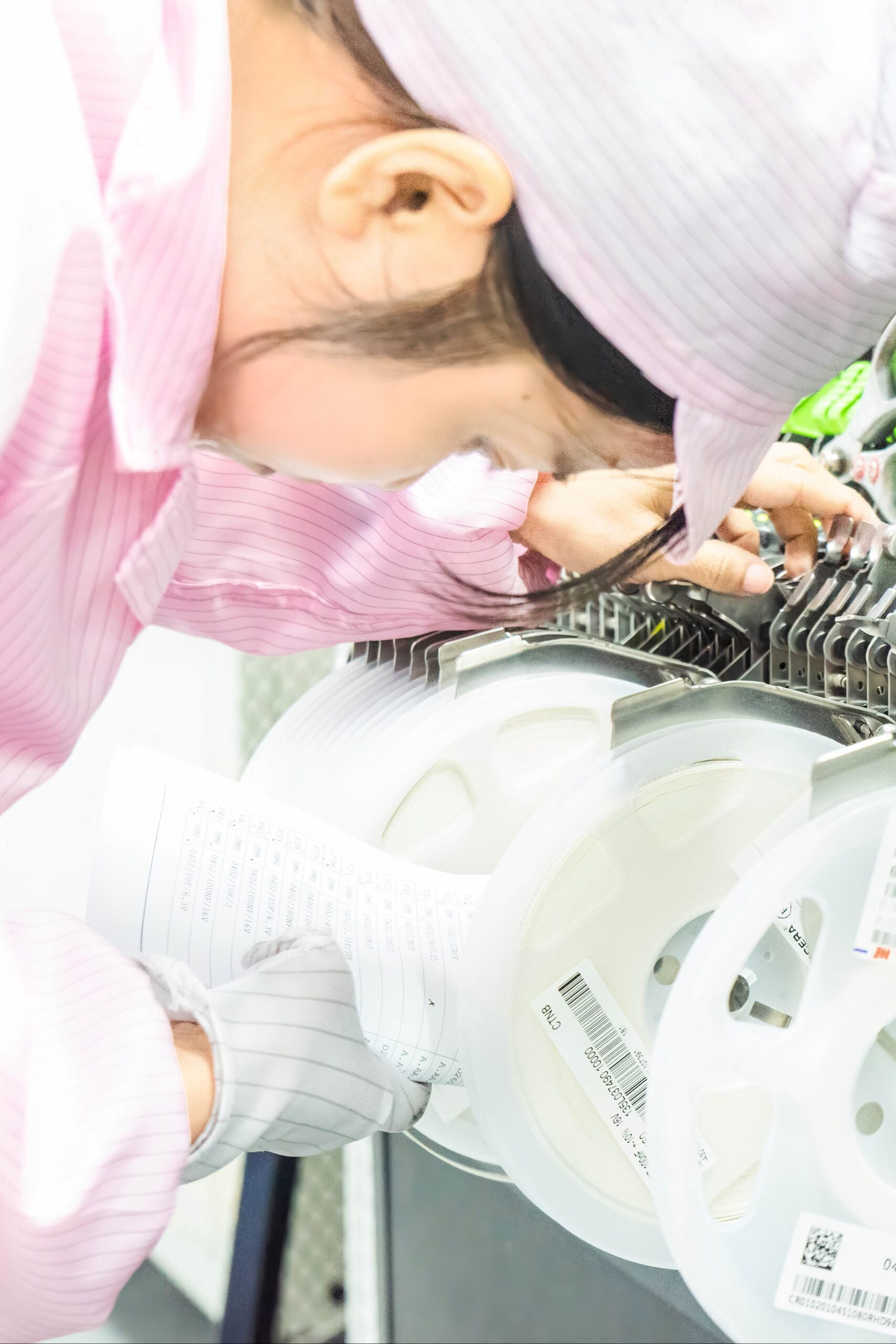
In this era of rapid technological development, medical equipment is becoming increasingly important for safeguarding human health. The PCBA (Printed Circuit Board assembly) inside the equipment, as its core component, has a direct impact on the performance and stability of the equipment due to the quality of its processing and assembly. Therefore, as purchasing personnel of electronic equipment manufacturers, it is particularly crucial to have a thorough understanding of each link in the processing and assembly of medical PCBA. Next, we will delve into this field together and conduct a detailed analysis of several core links in the processing and assembly of medical PCBA.
SMT Accuracy and Speed
In the processing of medical PCBA boards, the SMT soldering stage plays a crucial role. High-precision soldering machines can precisely install components, with the error controlled within 0.1mm or even less, ensuring the accuracy of component positions and significantly improving production efficiency. Moreover, the high-speed operation of the soldering machines fully demonstrates the pursuit of modern electronic manufacturing for efficient production.
Solder paste and Printing
Solder paste is a crucial material for fixing components, and its selection has a direct impact on product quality. Depending on the characteristics of different models and sizes of components, corresponding types of solder paste need to be selected. At the same time, in the solder paste printing process, it is necessary to ensure that the solder paste can be evenly and precisely printed onto the solder pads of the PCB, laying a solid foundation for the subsequent welding process.
Reflow Soldering and Temperature Control
Reflow soldering is the core process in SMT component assembly. By precisely controlling the temperature curve of the exhaust furnace, it is possible to ensure that the solder paste fully melts and forms a stable connection. An appropriate temperature curve not only affects the soldering quality but also effectively reduces the occurrence of welding defects and defective products.
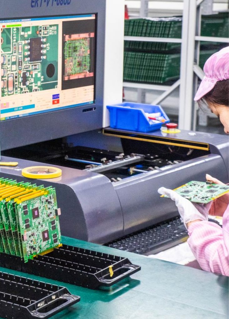
AOI Inspection and Quality Control
AOI (Automatic Optical Inspection) technology is widely used for detecting the welding quality. It uses optical inspection methods to visually inspect the completed PCB boards, and can promptly identify and report welding defects or errors, thereby providing strong support for ensuring the high quality and reliability of medical PCBAs.
Supplementary steps for DIP component processing
This process typically involves steps such as component insertion, wave soldering, and manual re-welding.
Functional testing and debugging
After completing the aforementioned processing steps, a functional testing and debugging phase is necessary. These tests cover multiple aspects such as ICT (in-line testing), FCT (function testing), and aging test, aiming to reveal any potential faults or hazards, thereby providing a clear direction for subsequent debugging and repair work.
Cleaning and coating
To enhance the protection and durability of the PCBA board, cleaning and coating processes are usually carried out after the processing is completed. Cleaning aims to remove the flux and other contaminants generated during the soldering process; while coating forms a protective film on the PCB surface to resist the adverse effects of humid, corrosive and other unfavorable environmental factors.
Unique Features of Medical PCB Circuit Board Assembly
The assembly of medical equipment PCB circuit boards requires high precision and reliability, a trend towards miniaturization and integration, the application of multi-layer boards and flexible boards, the application of lead-free soldering technology, the trend of automation and intelligent production, as well as strict quality control and inspection systems.
High precision and high reliability requirements
The assembly of components on the PCB circuit board of medical equipment must meet the requirements of high precision and high reliability. In the processes of component selection, soldering, and testing, strict quality control is necessary to ensure that the performance and stability of the components meet the standards.
The trend of miniaturization and integration
With the continuous upgrading and replacement of medical equipment, miniaturization and integration have become the development trend. This means that more components and functional modules need to be integrated onto the PCB circuit board, while maintaining the size and thickness of the circuit board within an acceptable range.
This imposes higher requirements on the packaging form and welding process of the components. For instance, smaller packaging dimensions, higher pin density, and more precise welding techniques are needed to achieve the miniaturization and integration of the circuit board.
The application of lead-free soldering technology
To meet environmental protection and health requirements, lead-free soldering technology has been widely applied in the assembly of PCB circuit board components for medical equipment. However, lead-free welding technology has higher requirements for welding processes and equipment. It necessitates precise control of welding temperature and duration to ensure welding quality and reliability.
The trend of automated and intelligent production
With the development of Industry 4.0 and intelligent manufacturing, automation and intelligence in production have become the development trend for the assembly of PCB circuit board components in medical equipment.
By employing technologies such as automated production lines, robots, and intelligent sensors, the assembly of components can be made automated, informationized and intelligent, thereby enhancing production efficiency and ensuring the stability of quality.
At the same time, we can also utilize technologies such as big data and cloud computing to conduct real-time monitoring and analysis of the production process, promptly identify and solve problems, and enhance the level of production management.
Strict quality control and inspection system
In order to ensure the quality and reliability of the assembly of medical equipment PCB circuit boards, a strict quality control and inspection system needs to be established. This includes strict quality control and management at all stages, from component procurement, welding process control, finished product inspection to after-sales service.
At the same time, advanced detection equipment and methods, such as X-ray detection and infrared thermal imaging detection, need to be employed to conduct a comprehensive inspection and evaluation of the circuit boards, ensuring that the quality and performance of the products meet the requirements.
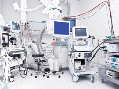
Medical PCBA Solution Samples
Medical Electronics: Ventilators, fascia guns, electrocardiographs (ECG), patient monitors, diagnostic devices.
| Device Type | Technical Solution | Validation Data |
| Cardiac Defibrillator | 6-Layer Rigid-Flex PCB | Survived 8,000G impact (-40~125°C cycling) |
| Surgical Arm | Metal-Core PCB | CTE matched titanium (6.8ppm/°C) |
| Portable Dialysis | Ceramic HF Board | Chemical resistance >8,000 hours |
| CGM Monitor | Polyimide Flexible PCB | Bend endurance >200,000 cycles |
| PET-CT Detector | Ultra-Low Loss Material | Dk tolerance ±0.03@100MHz |
Get a Medical PCBA Quote from JC Team
We stand behind the quality of our products with a comprehensive warranty.
- ISO 13485 medical device quality management system certification ensures full compliance with international standards throughout the entire process from design to production, complies with RoHS and REACH.
- We offer SMT, THT, and mixed-technology assembly capabilities to meet diverse design requirements and ensure optimal performance for complex medical PCBA applications.
- 100% full inspection including AOI optical inspection, X-RAY inspection (for detecting BGA solder joint void rate ≤5%), and flying probe testing, and the defect rate is controlled below 0.1%;
- Simulates the actual operating environment of medical devices through high-temperature and high-humidity (85℃/85% RH) aging tests, vibration and shock tests, etc.;
- We have the capability to manufacture multi-layer boards with 8 or more layers, meeting the strict requirements for signal integrity in medical imaging equipment;
- For medical-grade materials, we strictly select certified suppliers such as Murata and TDK to ensure that components meet biocompatibility and industrial-grade standards.
- Sterile products are manufactured in GMP-grade cleanrooms (such as clean environments with temperature controlled at ±1℃ and humidity at ±5%) and equipped with smart ESD prevention and control systems;
Why Choose JCPCBA for Your Medical PCB Assembly Needs?
- Quick Turn Prototype
- SMT/THT Assembly
- Mixed Assembly
- Lead Free Assembly
- Fast Turnaround PCB Assembly
- Prototype & High Volume
- 100% Electrical Testing
- Impedance control
- Blind,Buried and Plugged Vias
- BGA Assembly
- High-Temp,FR4,Flex,HDI,Rogers,etc
Privacy Protection:
Customer design files are confidential information. We strictly protect all information provided by our customers, ensuring your proprietary information is protected from disclosure, all data is secured and encrypted.
1-on-1 Service :
We taking full responsibility for every customer while offering dedicated 1-on-1 technical team support throughout the pre-sales, in-sales, and after-sales stages. During production, our 1-on- 1 sales will keep you updated of all the progress immediately enable you to master every detail of the production process.
Top Quality Guarantee:
100% electrical testing, AOI, IQC, OQC, and X-ray inspection for defect-free PCBs, which meet RoHS, ISO9001 standards and the standards of IPC Class II. We always react immediately if any issue and provide a quick solution. JC PCBA guarantee the quality, free maintenance and after-sales service for 2 years.
Fast, Efficient, No MOQ:
Generally, our PCB sample take 1-3 days, mass production takes 5-7 days, PCB assembly samples are completed in 10-15 days, and PCB assembly mass production is finished within 15-20 days. Besides, we have one fast sample line for urgent orders.
HOW TO GET A QUOTE: If you want to get a quick quotation for the PCB, please reach us at sales@pcbcustom.com.
Related Posts
Telecom PCBs Manufacturing: Printed Circuit Board in Telecommunication

Smart Home PCB Manufacturing & PCBA Services
Medical PCB Assembly and Manufacturing
LED PCBs: Building the Core of Efficient Lighting
Industrial PCBs Manufacturing & PCBA Services

Consumer Electronics PCBA Manufacturer – JCPCB
Automotive PCBs Manufacturing & PCBA Services