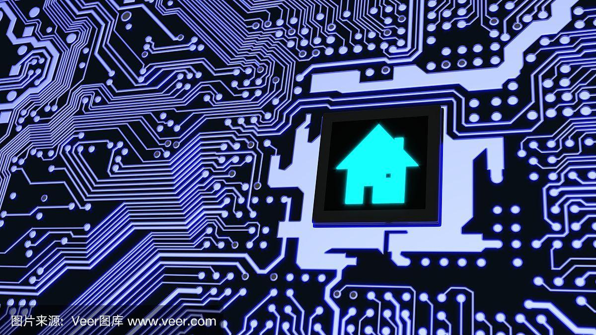
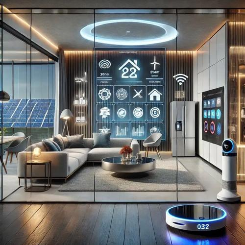
The concept of a smart house has finally become a reality, changing the way we live today. Smart home technology employs complicated technologies to assist us complete and simplify daily activities. Technology also saves energy and improves the comfort and security of homes. We can now utilize the lights to turn them on and off with a word of command, modify the temperature remotely, and keep a watch on the house when we leave—behind these seamless experiences lies a crucial component: the Smart Home PCB (Printed Circuit Board). This seemingly unassuming electronic component is actually the “nerve center” of smart home devices.
What is a Smart Home PCB?
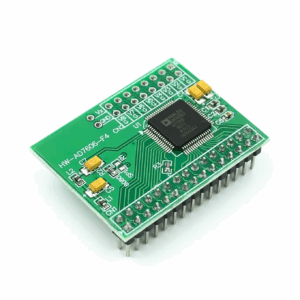
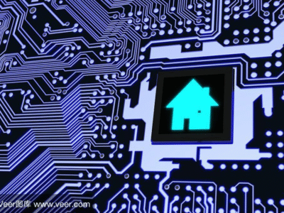
A Smart Home PCB is a printed circuit board specifically designed for smart home devices. It serves as the “stage” for electronic components like resistors, capacitors, and chips, responsible for signal transmission, power distribution, and data processing within the device. Unlike ordinary consumer electronics PCBs, it needs to adapt to complex home environments.
According to the definition by the Institute of Printed Circuits (IPC), Smart Home PCBs belong to specialized electronic interconnection components, whose design must meet the requirements for long-term reliable operation of smart home devices in environments with temperature and humidity fluctuations and complex electromagnetic conditions. Just like “house skeletons” customized for different apartment types, they are tailored to the functional needs of smart devices.
PCB Manufacturing Requirements for Smart Home PCBs
| Requirement | Description |
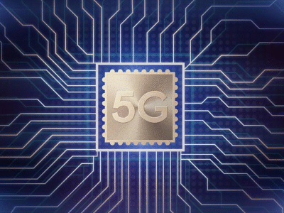
| High-Frequency PCB Design | Wi-Fi, Zigbee, Bluetooth modules |
| Multilayer Boards | 4+ layers for better EMI/EMC and compact design |
| High-Density SMT | 0603, 0402, 0201 components for compact boards |
| BGA Assembly | Common in MCU, camera modules, requiring X-ray inspection |
| Functional Testing Fixtures | Custom test for assembled boards |
| Small Batch & Quick Turn | Rapid prototyping for new product launches |
Comparison of Different Types of Smart Home PCBs
Classified by application scenarios, Smart Home PCBs mainly fall into three categories. Let’s use a “parameter card” for an intuitive comparison:
| Type | Typical Size | Layers | Operating Temp | Protection Class | Core Features | Representative Devices |
| Sensor Type | 20x20mm | 2-4 | -40~85℃ | IP65 | Low power consumption, high-precision signal acquisition | Temperature/humidity sensors, motion detectors |
| Control Type | 50x50mm | 4-6 | -20~70℃ | IP44 | Equipped with MCU, multi-interface integration | Smart switches, curtain controllers |
| Communication Type | 30x40mm | 6 | -30~75℃ | IP54 | High-speed wireless transmission, anti-interference | Smart gateways, WiFi modules |
Sensor-type PCBs are like “tactile nerves,” responsible for capturing environmental changes; control-type PCBs act as “brain centers,” processing instructions and sending action signals; communication-type PCBs serve as “messengers,” ensuring smooth data flow between devices.
Key Considerations in Smart Home PCB Design
Designing smart home PCBs isn’t just about drawing circuits. These key points directly affect device performance:
- Environmental adaptability is fundamental: Home environments have significant temperature and humidity variations, with inevitable dust and oil. PCBs should use conformal coating, and their operating temperature range is recommended to cover -40~85℃. In humid areas, anti-mold design is particularly important.
- Electromagnetic Compatibility (EMC) is essential: Household appliances like microwaves and refrigerators generate electromagnetic interference. The Institute of Electrical and Electronics Engineers (IEEE) recommends adding a ground plane in PCB layout, with a distance of at least 5cm between sensitive circuits and power circuits to avoid “device conflicts.”
- Power consumption control needs precision: Most smart home devices are battery-powered, so low-power design is crucial. Sleep Mode can be adopted to reduce MCU power consumption to ≤10μA during idle time, extending battery life.
- Interface compatibility should be considered: Reserve universal interfaces like USB and GPIO for future upgrades. For example, smart socket PCBs with reserved temperature and humidity sensor interfaces can be easily upgraded to products with environmental monitoring functions later.
Core Functions of Smart Home PCBs
Smart Home PCBs function as “all-rounders,” with these main capabilities:
- Signal acquisition is “perceptual ability”:
By connecting temperature, humidity, light, and other sensors, it converts physical signals into electrical signals. For instance, smart flowerpot PCBs collect soil moisture data in real-time.
- Data processing is “thinking ability”:
The equipped Microcontroller Unit (MCU) analyzes and calculates collected signals. Like smart door lock PCBs verifying whether fingerprint data matches authorized users.
- Instruction execution is “action ability”:
It receives processed instructions to control device operation. For example, smart curtain PCBs drive motor forward/reverse rotation to achieve opening and closing.
- Wireless communication is “social ability”:
Integrating WiFi, Bluetooth, and other modules to connect with mobile apps or gateways. Communication PCBs with data transmission rate ≥150Mbps can achieve command response delay ≤200ms.
- Status feedback is “reporting ability”:
It informs users of device status through indicator lights or data uploads. For example, smart air conditioner PCBs synchronize real-time temperature to the app.
FAQ: Answers to Your Concerns
Q1: What’s the difference between Smart Home PCBs and ordinary PCBs?
A: The biggest differences lie in environmental adaptability and functional integration. The former is optimized for protective and anti-interference designs in complex home environments, with more dedicated interfaces and low-power modules integrated.
Q2: How long is the lifespan of a Smart Home PCB?
A: Under normal use, it can reach 5-10 years. High-quality PCBs certified by the IPC-A-600G standard and using immersion gold technology can effectively resist oxidation and corrosion.
Q3: Do I need to pay attention to PCB parameters when purchasing smart home devices?
A: Ordinary users don’t need to delve into details, but they can indirectly judge PCB quality through device-labeled “operating temperature range” and “protection class.” For example, users in northern regions can choose devices with -40℃ low-temperature tolerance.
Why Choose JCPCBA for Your Smart Home PCB Assembly Needs?
- Quick Turn Prototype
- SMT/THT Assembly
- Mixed Assembly
- Lead Free Assembly
- Fast Turnaround PCB Assembly
- Prototype & High Volume
- 100% Electrical Testing
- Impedance control
- Blind,Buried and Plugged Vias
- BGA Assembly
- High-Temp,FR4,Flex,HDI,Rogers,etc
Top Quality Guarantee:
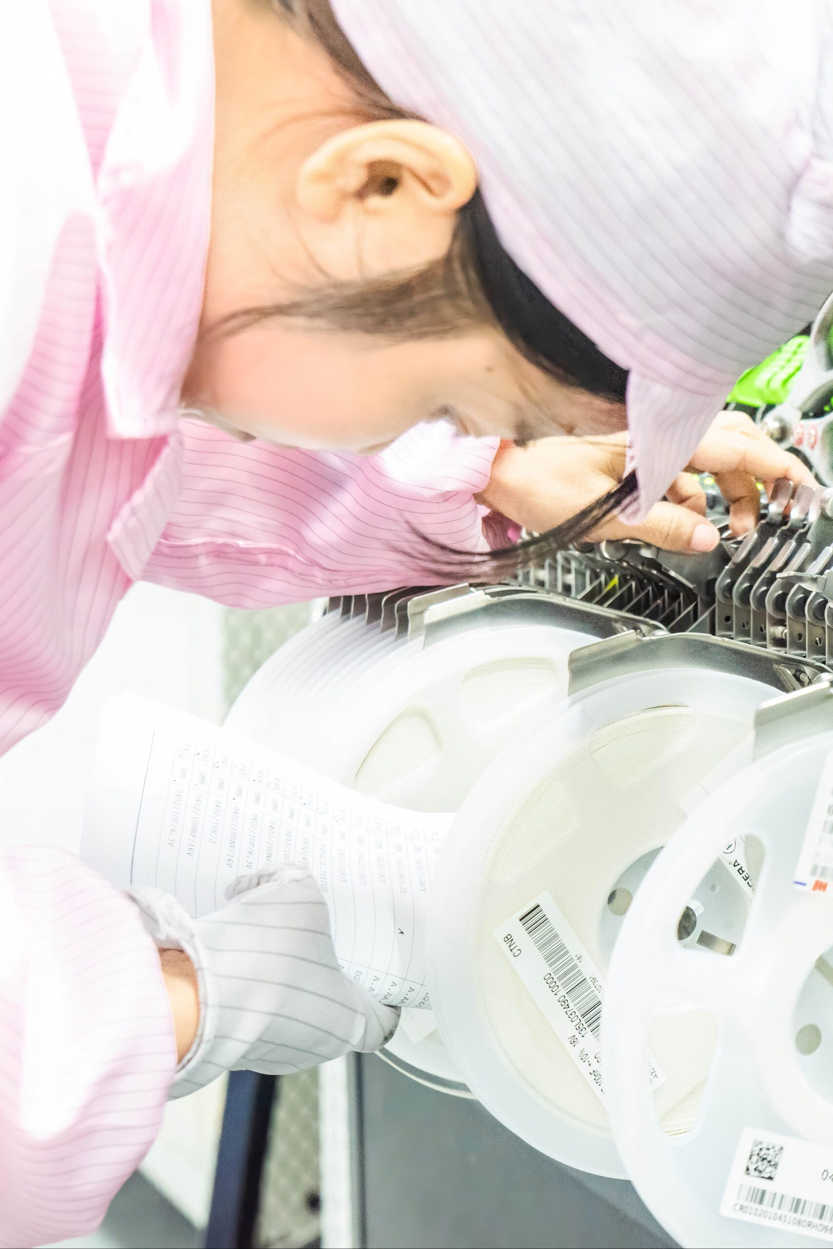
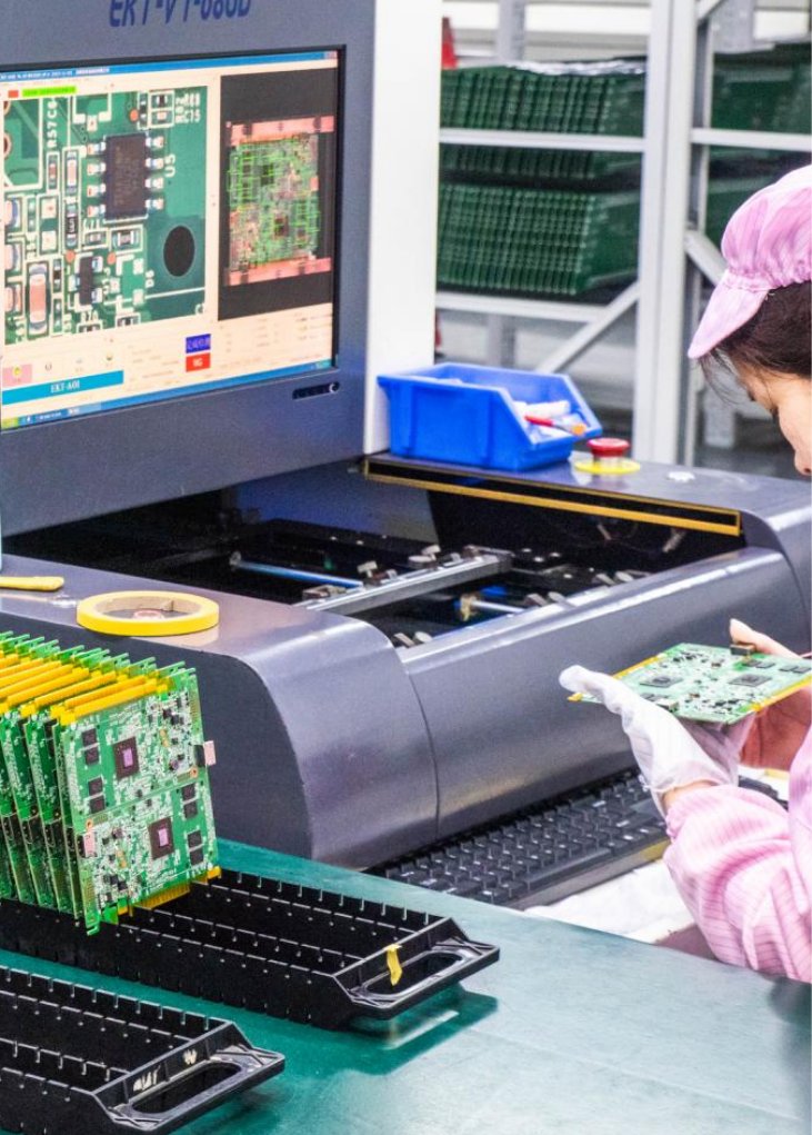
100% electrical testing, AOI, IQC, OQC, and X-ray inspection for defect-free PCBs, which meet RoHS, ISO9001 standards and the standards of IPC Class II. We always react immediately if any issue and provide a quick solution. JC PCBA guarantee the quality, free maintenance and after-sales service for 2 years.
Privacy Protection:
Customer design files are confidential information. We strictly protect all information provided by our customers, ensuring your proprietary information is protected from disclosure, all data is secured and encrypted.
1-on-1 Service :
We taking full responsibility for every customer while offering dedicated 1-on-1 technical team support throughout the pre-sales, in-sales, and after-sales stages. During production, our 1-on- 1 sales will keep you updated of all the progress immediately enable you to master every detail of the production process.
Fast, Efficient, No MOQ:
Generally, our PCB sample take 1-3 days, mass production takes 5-7 days, PCB assembly samples are completed in 10-15 days, and PCB assembly mass production is finished within 15-20 days. Besides, we have one fast sample line for urgent orders.
HOW TO GET A QUOTE: If you want to get a quick quotation for the PCB, please reach us at sales@pcbcustom.com.
Conclusion
Although hidden inside devices, Smart Home PCBs are the “unsung heroes” of smart home experiences. From accurately perceiving environmental changes to stably executing user instructions, every design detail affects our quality of life. As smart homes move toward AI integration and low-power consumption, Smart Home PCBs will also undergo smarter upgrades. Next time you use a smart device, take a moment to appreciate the silent dedication of this “invisible steward”!
Related Posts
Telecom PCBs Manufacturing: Printed Circuit Board in Telecommunication
Smart Home PCB Manufacturing & PCBA Services
Medical PCB Assembly and Manufacturing
LED PCBs: Building the Core of Efficient Lighting
Industrial PCBs Manufacturing & PCBA Services

Consumer Electronics PCBA Manufacturer – JCPCB
Automotive PCBs Manufacturing & PCBA Services