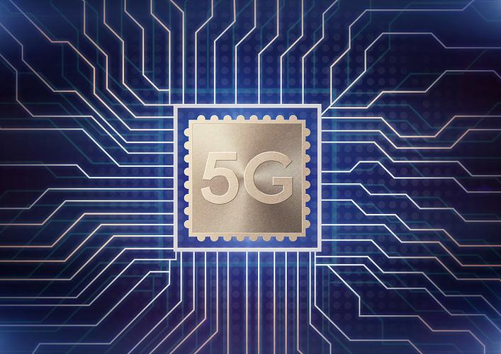
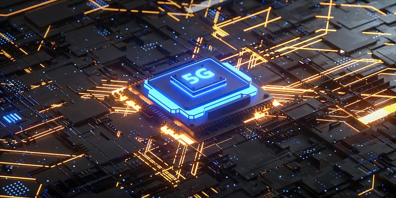
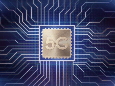
In today’s hyper-connected world, where 5G networks are spreading rapidly and 6G research is accelerating, telecommunication equipment operates at unprecedented speeds and frequencies. Behind these powerful devices lies a critical component: the Telecommunication PCB. As the “nervous system” of telecom equipment, it ensures stable signal transmission, efficient power management, and reliable operation even in harsh environments.
What is Telecommunication PCB?
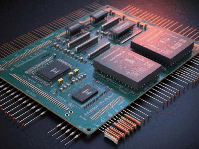
Telecommunication PCB (Printed Circuit Board) is a specialized circuit board designed for telecommunication equipment that requires high-speed signal transmission, low signal loss, and stable performance in complex electromagnetic environments. Unlike regular PCBs used in consumer electronics, telecom PCBs are engineered to handle frequencies ranging from hundreds of MHz to tens of GHz, with strict control over signal integrity and electromagnetic compatibility (EMC).
According to IPC (Association Connecting Electronics Industries) standards, telecom PCBs typically meet higher performance criteria, including tighter impedance control (±10% tolerance), lower dielectric loss (Df < 0.002 at 10 GHz), and better thermal conductivity (≥1.5 W/m·K). These parameters ensure they can support the high-data-rate requirements of modern telecom networks.
Applications of Telecommunication PCB
Wireless Networking.
- Telecom infrastructure.
- Space communications technology.
- Satellite Communication Systems
- Mobile devices.
- Network management system.
- Wireless Communication Systems
- Signal boost online systems.
- Integrated Voice and Data Systems (VoIP)
- PBX systems.
- Phone switching systems.
- Cell transmissions and tower electronics.
- High-speed routers and servers.
Critical Production Considerations
Material Compatibility:
Ensure substrate and prepreg have matching thermal expansion coefficients to prevent warpage.
Signal Integrity:
Maintain consistent trace width/spacing and avoid right-angle bends in high-frequency paths.
Thermal Management:
Incorporate thermal vias and copper pours to dissipate heat from power components.
Key Functions of Telecommunication PCB
- Signal Transmission: Enable high-speed, low-loss transfer of analog and digital signals.
- Power Management: Distribute stable power to various components while minimizing noise.
- Thermal Regulation: Dissipate heat generated by high-power components like RF amplifiers.
- Mechanical Support: Provide structural stability for sensitive telecom components.
- EMC Assurance: Maintain signal integrity in noisy electromagnetic environments.
Types of Telecommunication PCB
| PCB Type | Key Features | Typical Applications | Advantages |
| High-Frequency PCB | Dk 3.0-4.5, low Df, PTFE/ceramic substrates | 5G base stations, radar systems | Minimal signal loss at high frequencies |
| High-Speed PCB | Controlled impedance (50-100Ω), low crosstalk | Data center switches, routers | Supports >10 Gbps data rates |
| Rigid-Flex PCB | Combination of rigid and flexible substrates | Portable telecom devices, satellite modules | Space-saving, vibration-resistant |
| Heavy Copper PCB | 3-20 oz copper layers | Power amplifiers, battery management | Excellent heat dissipation, high current capacity |
Design Considerations for Telecommunication PCB
- EMI/EMC Design: Use ground planes, shielding cans, and filter components to reduce electromagnetic interference.
- Power Distribution: Design star-shaped power distribution networks to minimize voltage drops.
- Component Placement: Separate analog/RF sections from digital sections to prevent interference.
- Thermal Simulation: Use tools like ANSYS Icepak to optimize heat dissipation paths before prototyping.
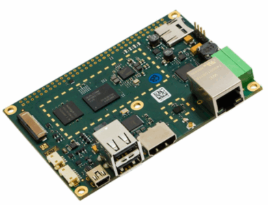
Telecommunication PCB Solution Example: 5G Base Station PCB
- Our 5G base station PCB solution features:
- 12-layer stackup with Rogers 5880 (Dk 2.2) and FR-4 hybrid substrate
- Impedance-controlled differential pairs (85Ω ±5%) for RF signals
- Embedded heat spreaders with 2 oz copper layers
- Laser microvias (50μm diameter) for high-density interconnects
- Operating temperature range: -40℃ to 125℃
- Compliance with 3GPP TS 38.101 standards for 5G NR frequency bands
This solution reduces signal loss by 30% compared to traditional FR-4 PCBs and supports 28 GHz mmWave frequencies, making it ideal for 5G mid-band and high-band applications.
FAQ About Telecommunication PCB
Q: What’s the difference between telecom PCB and regular PCB?
A: Telecom PCBs require stricter impedance control, lower signal loss, and better EMC performance to handle high-frequency signals in telecom networks.
Q: How does 5G affect telecom PCB requirements?
A: 5G’s higher frequencies (sub-6 GHz and mmWave) demand lower dielectric loss, tighter tolerances, and improved thermal management compared to 4G PCBs.
Q: What substrate materials are best for high-frequency telecom PCBs?
A: PTFE-based materials (Rogers, Taconic) and ceramic-filled laminates offer the low Dk and Df needed for high-frequency applications.
Q: How long does it take to produce a custom telecom PCB?
A: Prototypes take 7-10 days, while mass production typically requires 2-4 weeks, depending on complexity.

Why Choose JCPCBA for Your telecommunication PCB Assembly Needs?
- Quick Turn Prototype
- SMT/THT Assembly
- Mixed Assembly
- Lead Free Assembly
- Fast Turnaround PCB Assembly
- Prototype & High Volume
- 100% Electrical Testing
- Impedance control
- Blind,Buried and Plugged Vias
- BGA Assembly
- High-Temp,FR4,Flex,HDI,Rogers,etc
Top Quality Guarantee:
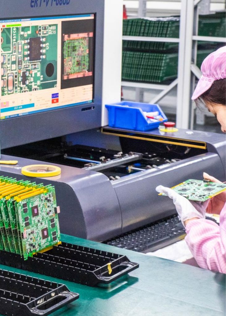
100% electrical testing, AOI, IQC, OQC, and X-ray inspection for defect-free PCBs, which meet RoHS, ISO9001 standards and the standards of IPC Class II. We always react immediately if any issue and provide a quick solution. JC PCBA guarantee the quality, free maintenance and after-sales service for 2 years.
Privacy Protection:
Customer design files are confidential information. We strictly protect all information provided by our customers, ensuring your proprietary information is protected from disclosure, all data is secured and encrypted.
1-on-1 Service :
We taking full responsibility for every customer while offering dedicated 1-on-1 technical team support throughout the pre-sales, in-sales, and after-sales stages. During production, our 1-on- 1 sales will keep you updated of all the progress immediately enable you to master every detail of the production process.
Fast, Efficient, No MOQ:
Generally, our PCB sample take 1-3 days, mass production takes 5-7 days, PCB assembly samples are completed in 10-15 days, and PCB assembly mass production is finished within 15-20 days. Besides, we have one fast sample line for urgent orders.
HOW TO GET A QUOTE: If you want to get a quick quotation for the PCB, please reach us at sales@pcbcustom.com.
Conclusion
Telecommunication PCBs enable the seamless operation of 5G networks, data centers, and satellite communication systems. As telecom technology advances toward 6G, the demand for high-performance, reliable PCBs will only grow.
Whether you need a custom solution for 5G base stations or high-speed data networking equipment, our team of experts is ready to deliver PCB solutions that meet your exact specifications. Contact us at sales@pcbcustom.com today!
Related Posts
Telecom PCBs Manufacturing: Printed Circuit Board in Telecommunication

Smart Home PCB Manufacturing & PCBA Services
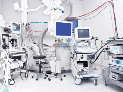
Medical PCB Assembly and Manufacturing
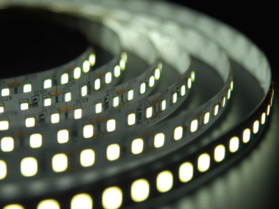
LED PCBs: Building the Core of Efficient Lighting
Industrial PCBs Manufacturing & PCBA Services

Consumer Electronics PCBA Manufacturer – JCPCB
Automotive PCBs Manufacturing & PCBA Services