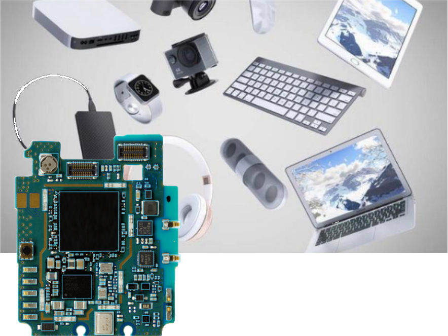
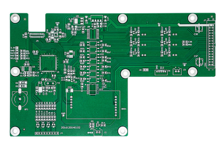
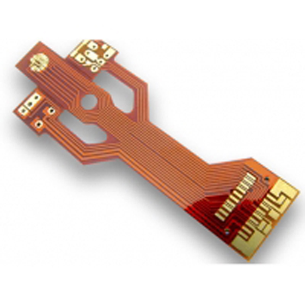
PCB Manufacturing
Top PCB Manufacturing Factory in China - CJPCB
Top automated lines which have real-time process monitoring, keeping quality steady every time.
CJ PCBA combines cutting-edge tech and top industry expertise. We deliver high-performance PCB surface finishes which meeting the toughest specs, and 24H fast delivery. We have advantage to supply single to multilayer FR4 PCB, Aluminum PCB, Flexible Polymind PCB, Impedance Control PCB, Buried&Blind Holes PCB and etc. Our diverse processes ensure optimal solderability, durability and electrical performance. They suit many uses—from consumer electronics to aerospace systems.
PCB DELIVERY SCHEDULE
Accelerating your projects with fast turnaround times and short lead times for quick delivery.
SAMPLES PCB |
QUICK SAMPLE |
MASS PRODUCTIONS |
---|---|---|
1-2L: 2-3 DAYS |
1-2L: 3-7 DAYS |
1-2L: 3-7 DAYS |
4-8L: 2-7 DAYS |
4-8L: 7-10 DAYS |
|
10-18L:4-9 DAYS |
10-18L:10-15 DAYS |
PCB Manufacturing Capabilities
We offer manufacturing of rigid, flexible, rigid-flexible, and aluminum boards, and supporting one – stop, rapid – turnaround PCB assembly solutions. We have experience in manufacturing PCB from single layer till 58layers , 24H fast delivery. FPC can be 1 layer till 6layers.

Rigid PCB(1-58L )

Flex PCB (1-6L)

Rigid-Flex PCB(2-10L)

Aluminum/Copper PCB(1-2L )
Surface Finish
Standard tin spraying, Lead-free tin spraying, Immersion gold, Electroplated nickel-gold, Electroplated hard gold, OSP, Immersion silver, Immersion tin, or Composite processes.

Gold plating(ENIG)

LF-HASL(Lead-Free)

OSP(Antioxidant)

Immersion Silver

Immersion Tin
Our Commitment to Quality
Committing to rigorous quality assurance measures to deliver products that exceed industry standards.
PCB Raw Material
Our PCB boards use genuine Grade-A materials, such as Jian Tao (KB) and Nanya (NY). Good dimensional stability after heating. Curvature of the board ≤0.75%, Not easy to deformation and plate warping; The copper coating on the hole wall has better adhesive force; no layered or drape in copper. Drilling Roughness ≤25.4UM.
Technology Standard
Standard copper PTH technic makes copper in vias reach 20-22UM. Even better than IPC class 2 requirement (via copper thickness 18-20UM). lesser risk of copper shedding in faults and holes when under high current or high temperature.
Solder Mask
High-quality solder mask inks from brands like Ronda are applied using a photosensitive process. Glossy ink, strong color. Solder resistance thickness up to standard 8-30UM. Help to achieve better filling via with resin and better adhesive force solder mask on your PCB.
Plating&Surface Treatment
Premium electroplating and surface treatment chemicals are employed to achieve a 100% yield rate. Lesser soldering problem, BGA solder risk, make sure copper in via, surface treatment has strictly control within IPC standard. The pollution and oxidation of the board surface, black nickel, abnormal nickel thickness, SCUM (shadow) and other problems are strictly controlled during the operation process.

6L ENIG 0.8mm

BGA pads

Circuits

Routing

Surface finish
Our PCB Fabrication Procedure
We adhere to the principle of prioritizing quality and service.
PCB production process
Pre – stack → Automatic sheets cutting →Inner pretreatment → lamination machine → Exposure →Developing machine → Layer etching → Drill machine → AOI testing → Solder mask ink → Silk screen → Detection → FQC → Packging
FPC production process
Engineering File Preparation → Copper Foil Drilling (PTH, Plated Through Hole) → Copper Plating → Pre-Treatment → Dry Film Lamination & Stamping → Exposure → Development → Etching → Film Stripping → AOI (Automated Optical Inspection) → Pre-Treatment → Coverlay Lamination or Ink Printing → Plating Pre-Treatment → Post-Plating Treatment → Surface Finish → Legend Printing → Electrical Testing → Laser Profiling → FQC (Final Quality Control) → Packaging & Shipment。

WHY PARTNER WITH CJPCBA?
Quality Assurance
Materials and PCB are manufactured in full compliance with customer specifications, ensuring alignment with your quality standards. Stringent quality control is implemented across all stages, resulting in a customer satisfaction rate of over 99%.
Speed & Reliability Service
We has built strategic partnerships with top logistics companies like DHL/FedEx. Ensuring timely deliveries with our speedy and reliable logistics services, keeping your supply chain smooth and efficient.
Rapid Turnaround
24–72-hour turnaround for urgent order. Our company has a complete production process and dedicated order-following personnel to follow up on delivery dates and provide timely feedback on production conditions to ensure on-time delivery.
Competitive price
With our in-house factory and professional team, we minimize intermediate costs to provide the competitive quotes. Optimizing your project’s budget and timeline with cost-effective strategies and efficient planning.
PCB FAQ
CAM350/Altium Designer/Genesis2000//PADS/GC-power.
Our company's engineering team offers free DFM analysis. All data will be reviewed and confirmed after production. If there are any issues, an EQ confirmation will be issued.
The electrical testing of PCBS mainly involves checking whether there are any open or short circuit issues on the PCB board and analyzing whether it matches the customer's design data.
CTI stands for Tracking Index, which is the voltage at which marks are left on the surface of a board when it leaks and burns. For conventional FR4 boards, the CTI value is PLC3, that is, 175<CTI<245.
For finished plate thickness less than 1mm, it can be controlled at +/-0.1mm. For finished plate thickness greater than 1mm, the strictest control can be +/-0.13mm. Normally, it is controlled at +/-10%. (Because the plates and materials such as pp have certain tolerances, and the chip tolerance close to +/-0.075mm).
How to order
Please send your relevant design documents (such as Gerber/Bom) and requirements. We strictly protect all information provided by our customers. Send us:sales@pcbcustom.com
You will receive feedback from a dedicated salesperson providing one-on-one service throughout your entire process within 6 hours and a customized quotation within 24 hours.
After fully understanding the customer's requirements and confirming the price, lead time, payment method, transportation and qualification certification, sign the PI agreement and make prepayment.
After receiving prepayment, production will be arranged immediately. During the production process, your full-time salesperson will proactively report the production progress to you. Before shipment, detailed photos, test videos and packaging of the products will be taken for your confirmation.
We will always react immediately if there is any issue and provide a quick solution. CJ PCBA guarantee the quality and after-sales service for 2 years. If everything well, we will welcome further cooperation.
Our Testimonials

PCB&Assembly
Everything is good, PCBs work good by now, thank you(Gracias)! To CJ Teams.

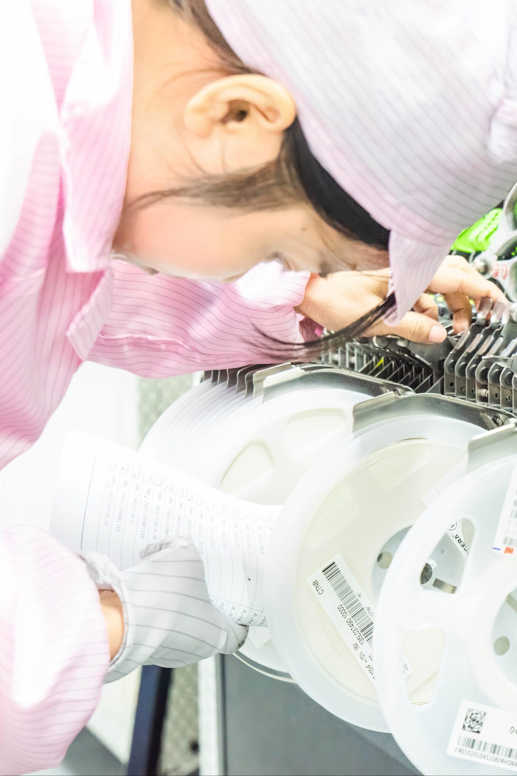
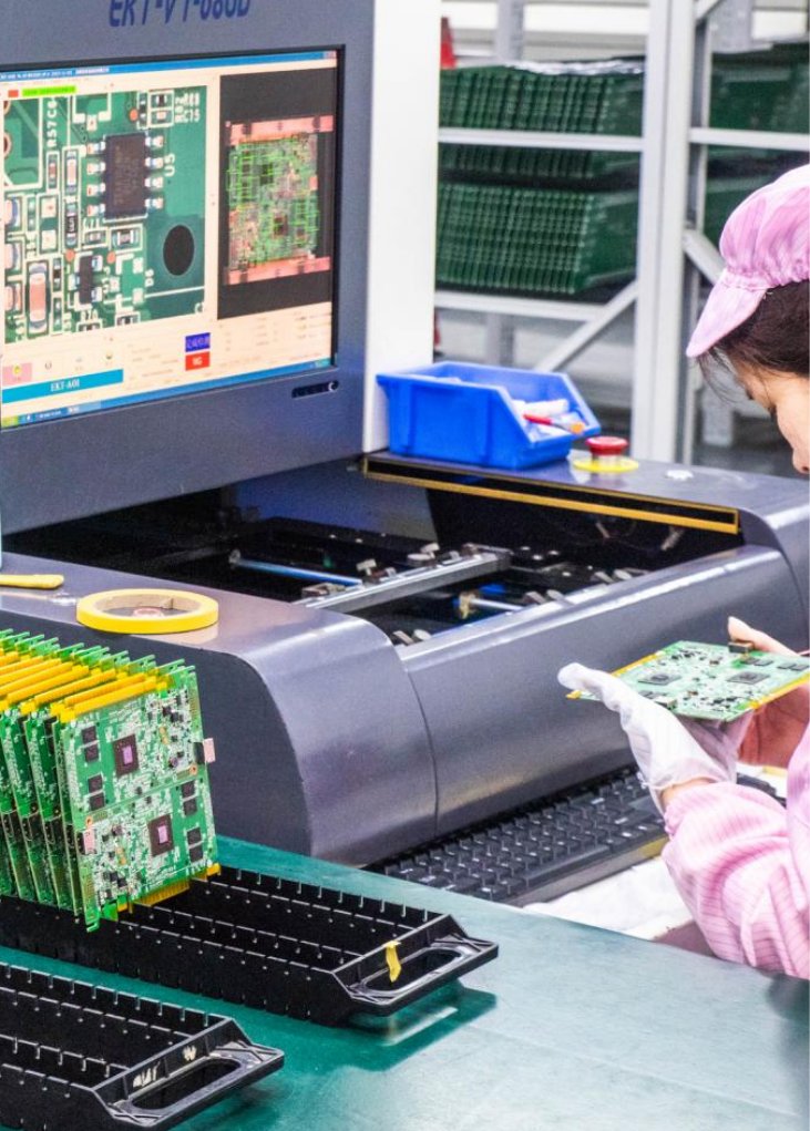
PCBA programming,conformal coating,testing.
The boards are prefect, I am really happy to receive my boards, the components are really good!
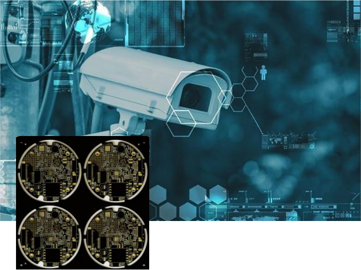
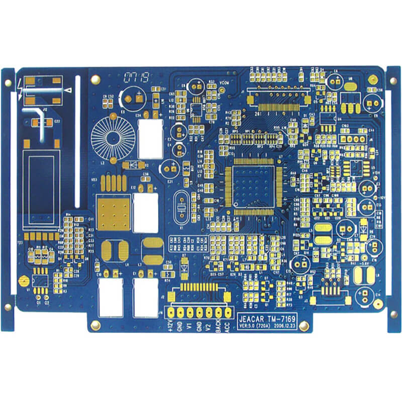
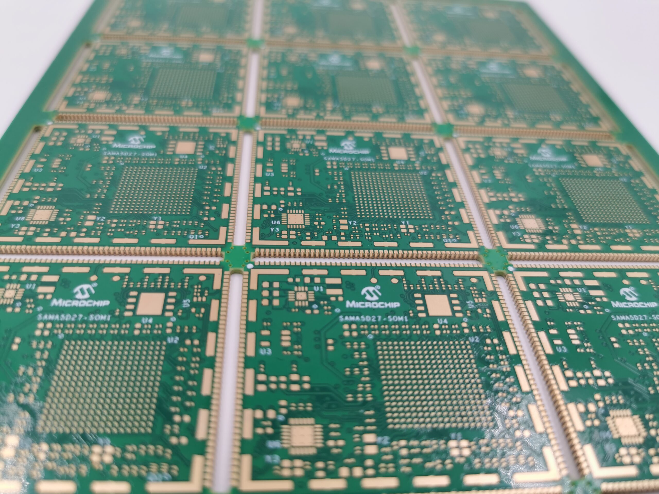
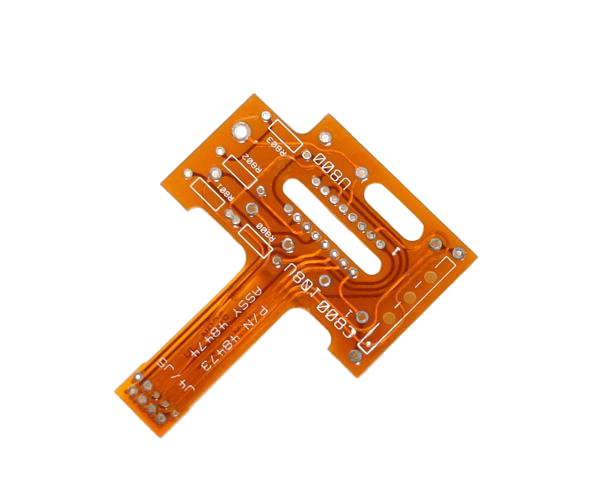
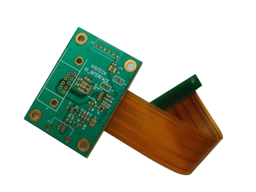
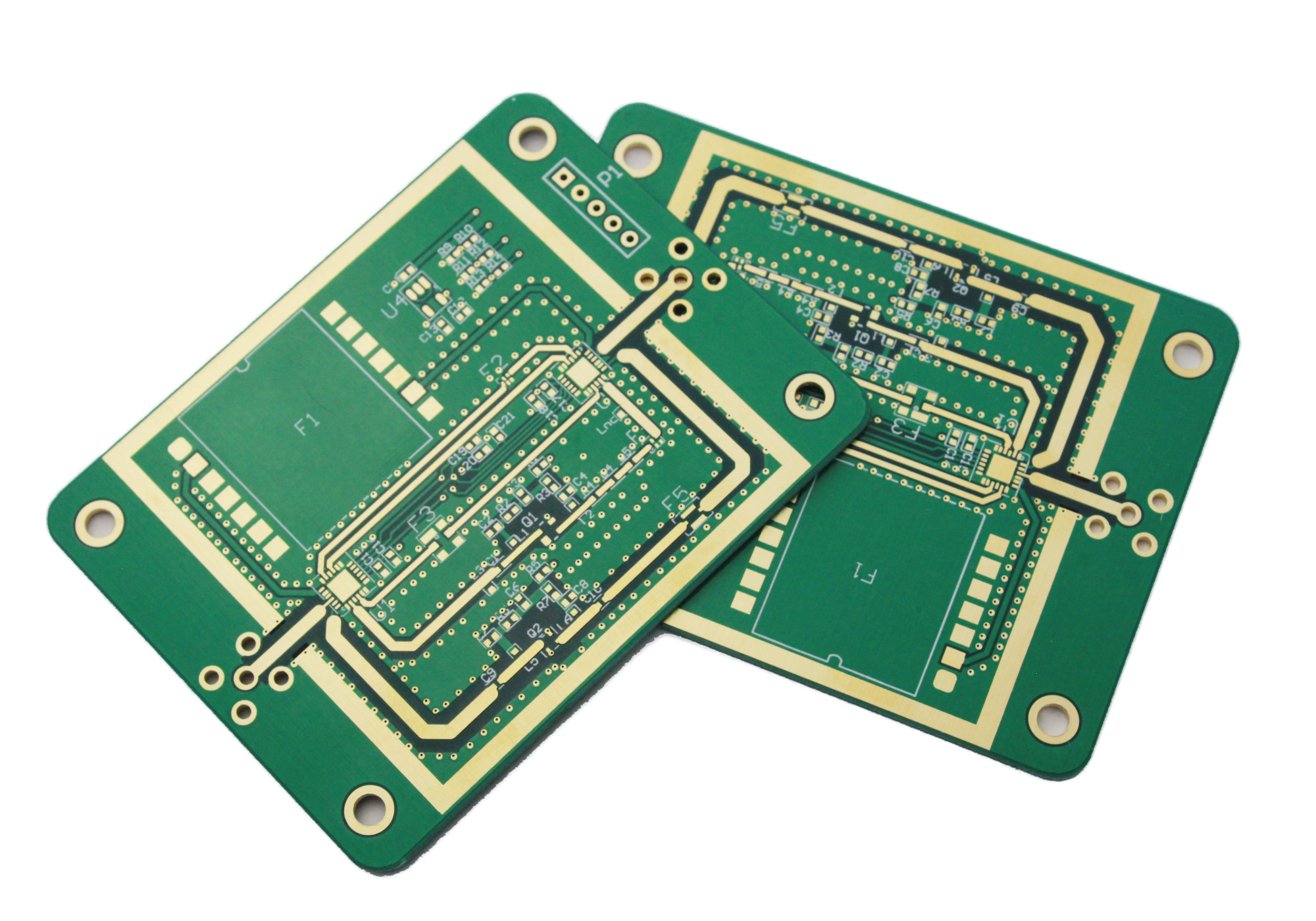
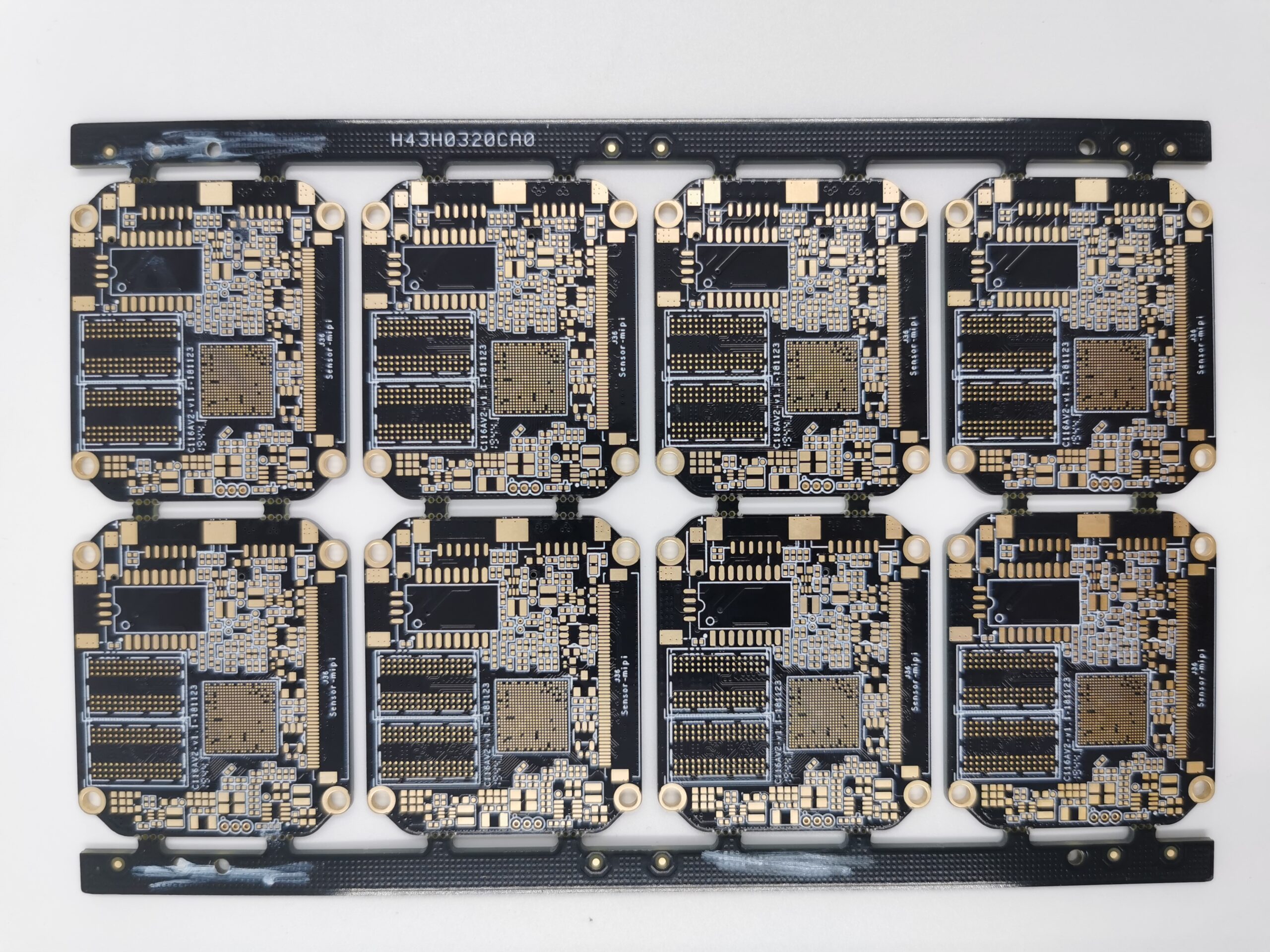
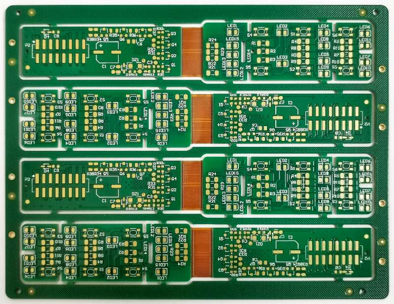
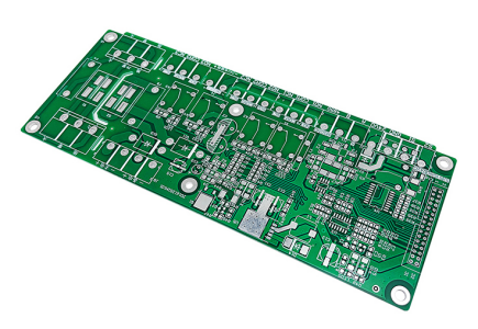
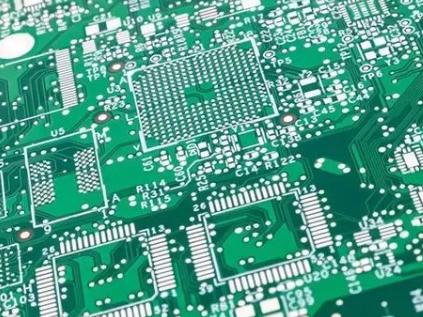
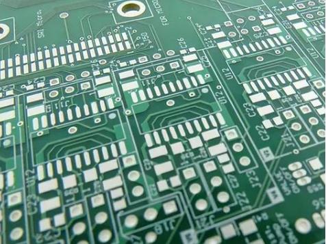
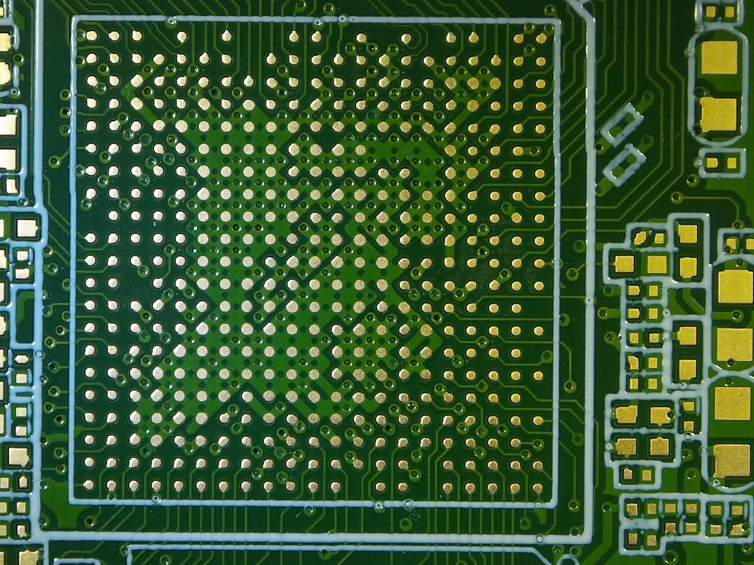
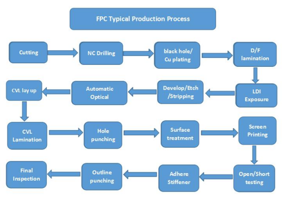
PCB Manufacturing
Uploaded my Gerber files, got a quote in hours, and parts arrived sooner than quoted. Nice.”

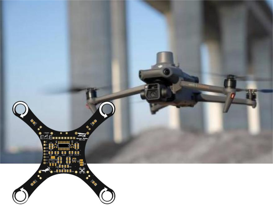
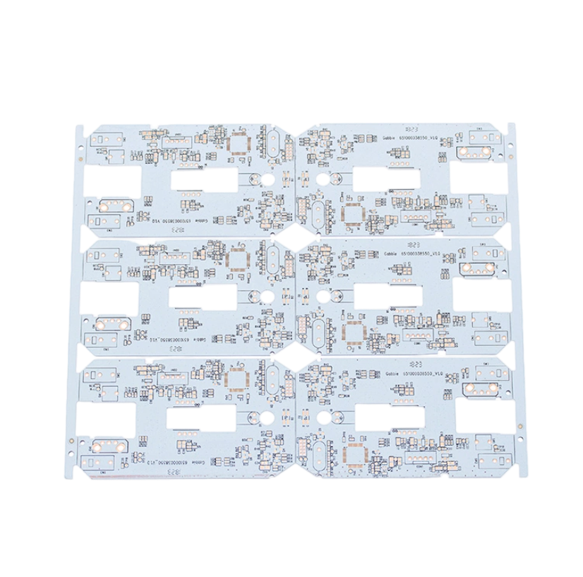
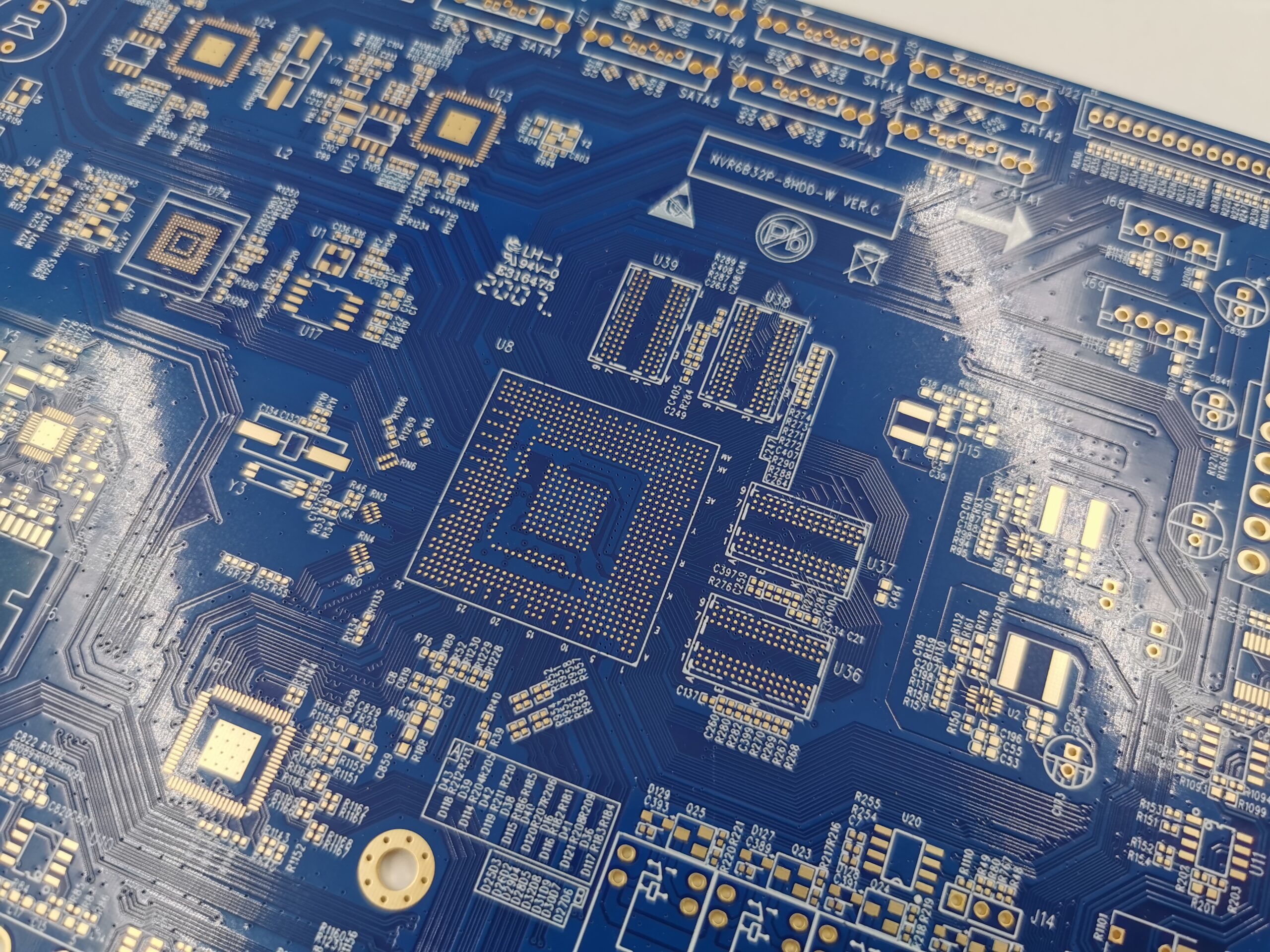
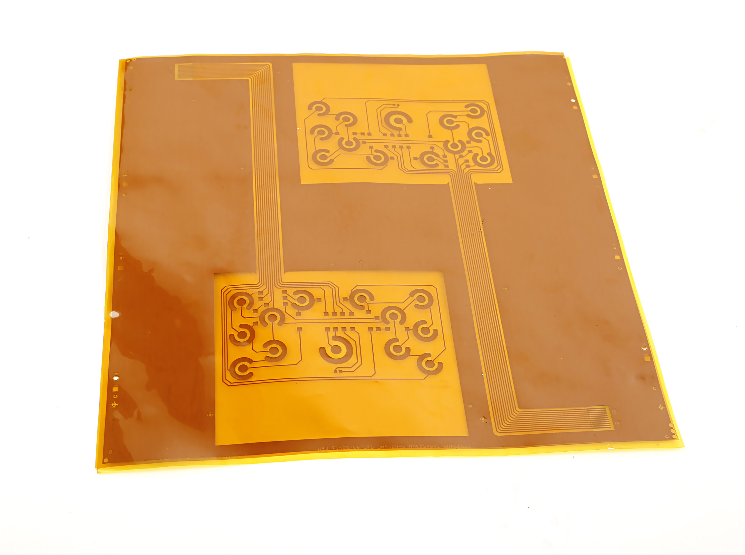
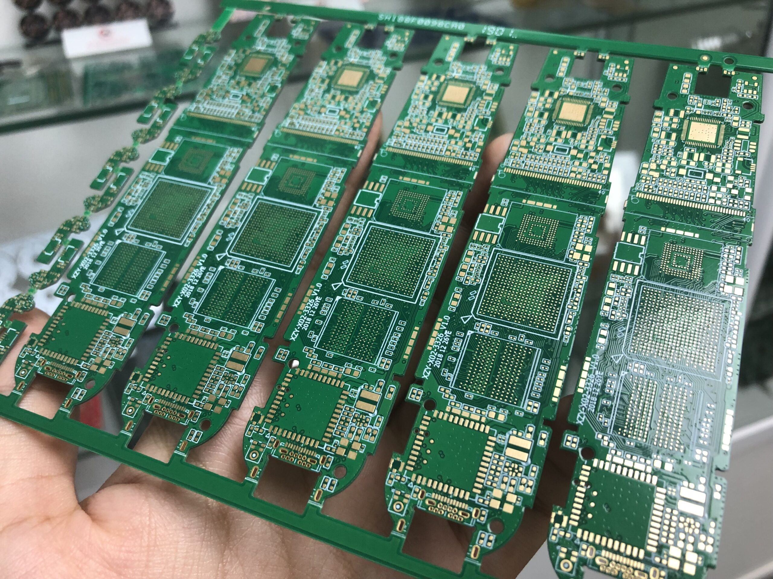
PCBA Prototyping& Batch production
I am happy to find you(Jason)!No minimum order hassle, and the soldering looks good, cleanly well.

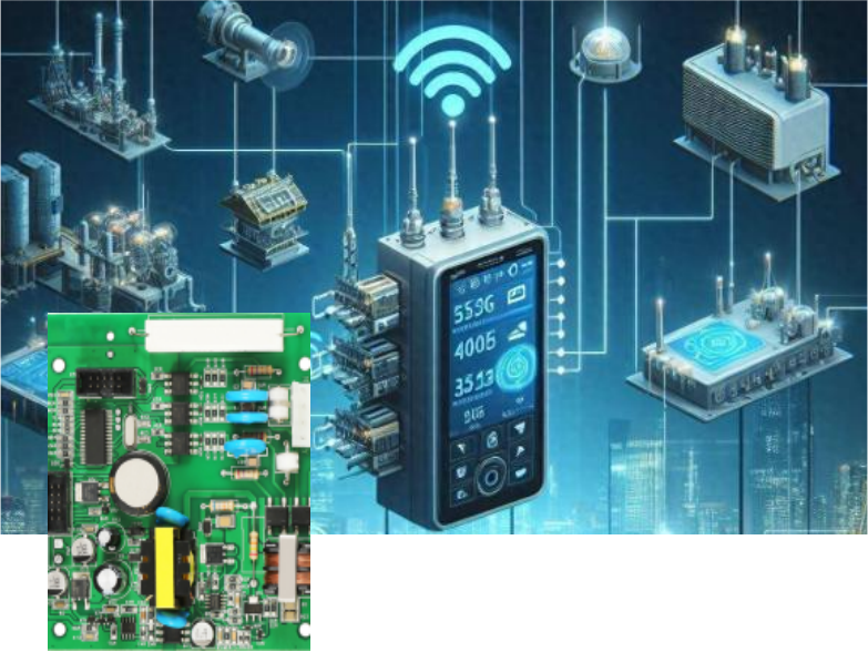
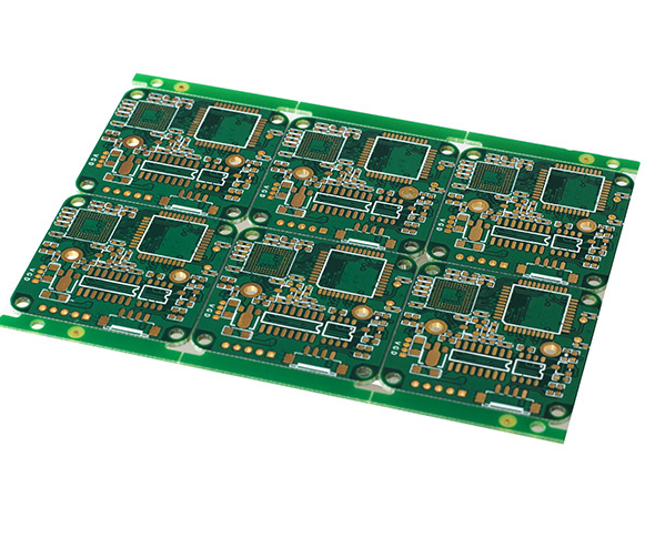
PCBA and components and modules.
We tested all, PCBs works well, thank you! Michael.
Our PCBA Solutions Across Industries
safety protection, electrical appliances, digital home appliances, and more.
Contact Us
Help you easily achieve your electronic product.
Headquarter Address
SEG Plaza 4406A,No. 1002, Huaqiang North Road,Fuqiang Community, Huaqiang North Street, Futian District. Shenzhen
Factory Address
1st Floor, Building H, Tangxi No.2 Industrial Zone, Xijing Road, Gushu, Bao’an District, Shenzhen
Phone
+86-755-85122468
sales@pcbcustom.com
Get Free Quote
Our 1-on-1 sales engineer will reply as soon as possible and quote you within one day!

