-
 100% Original
-
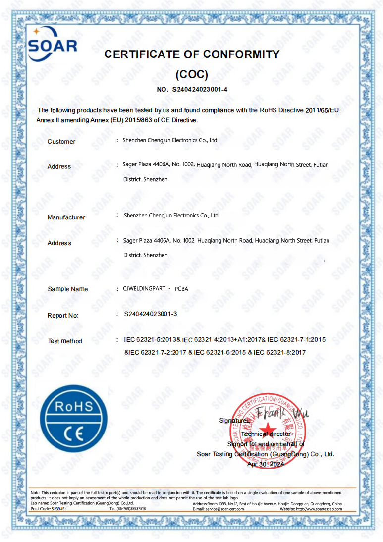
Anti-counterfeit
-
Speed Delivery
-
ISO9001
-
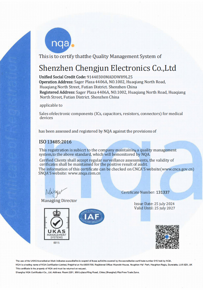
ISO13485
-
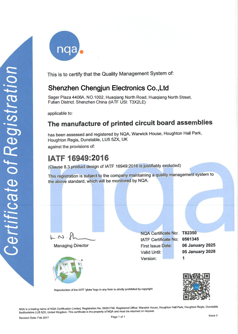
IATF16949
-
INNER:
-
OUTER:
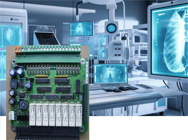
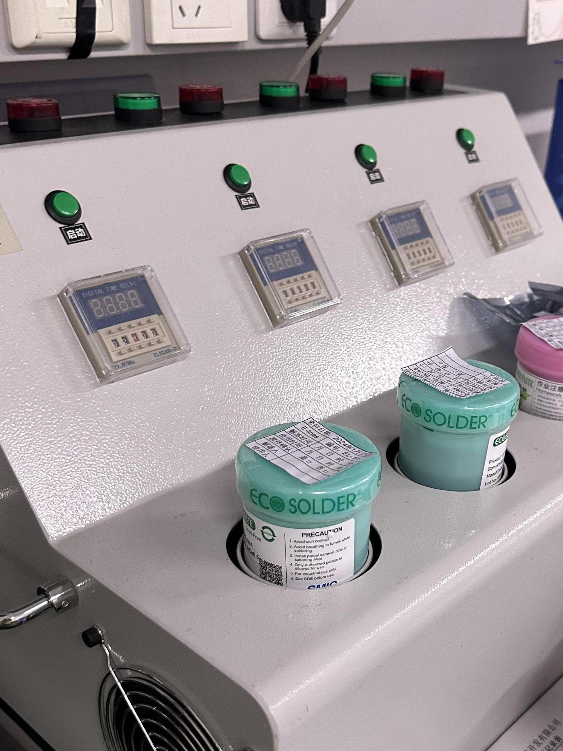
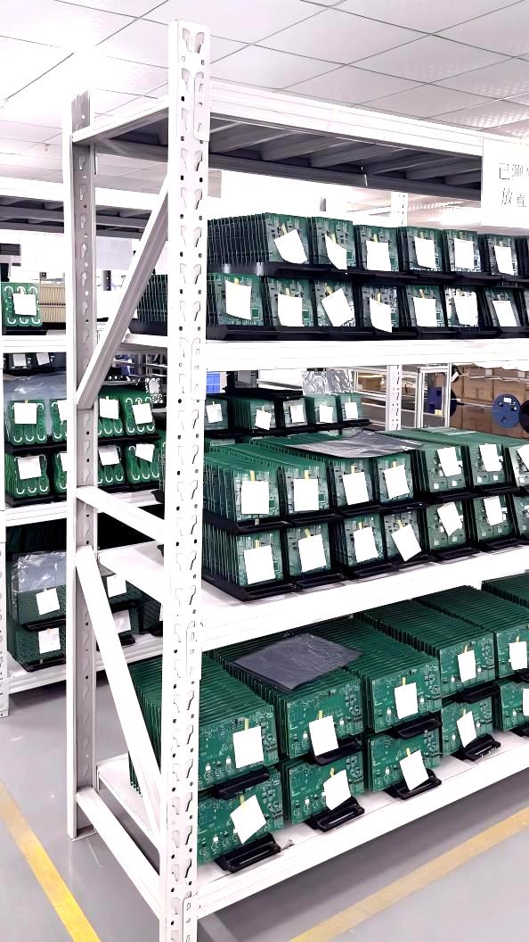
PCB&Assembly
Everything is good, PCBs work good by now, thank you(Gracias)! To JC Teams.
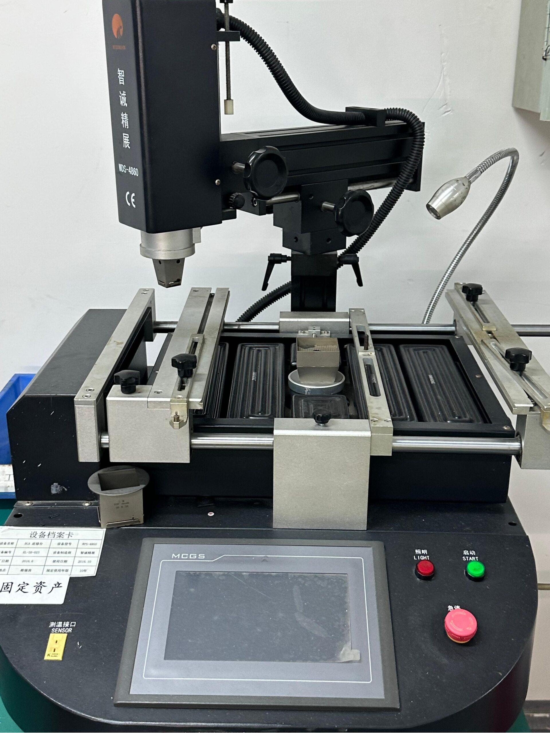
PCBA programming,conformal coating,testing.
The boards are prefect, I am really happy to receive my boards, the components are really good!
3D Printing&Injection Molding
I am very pleased to work with you(Sulin)! It feels like you are a professional!
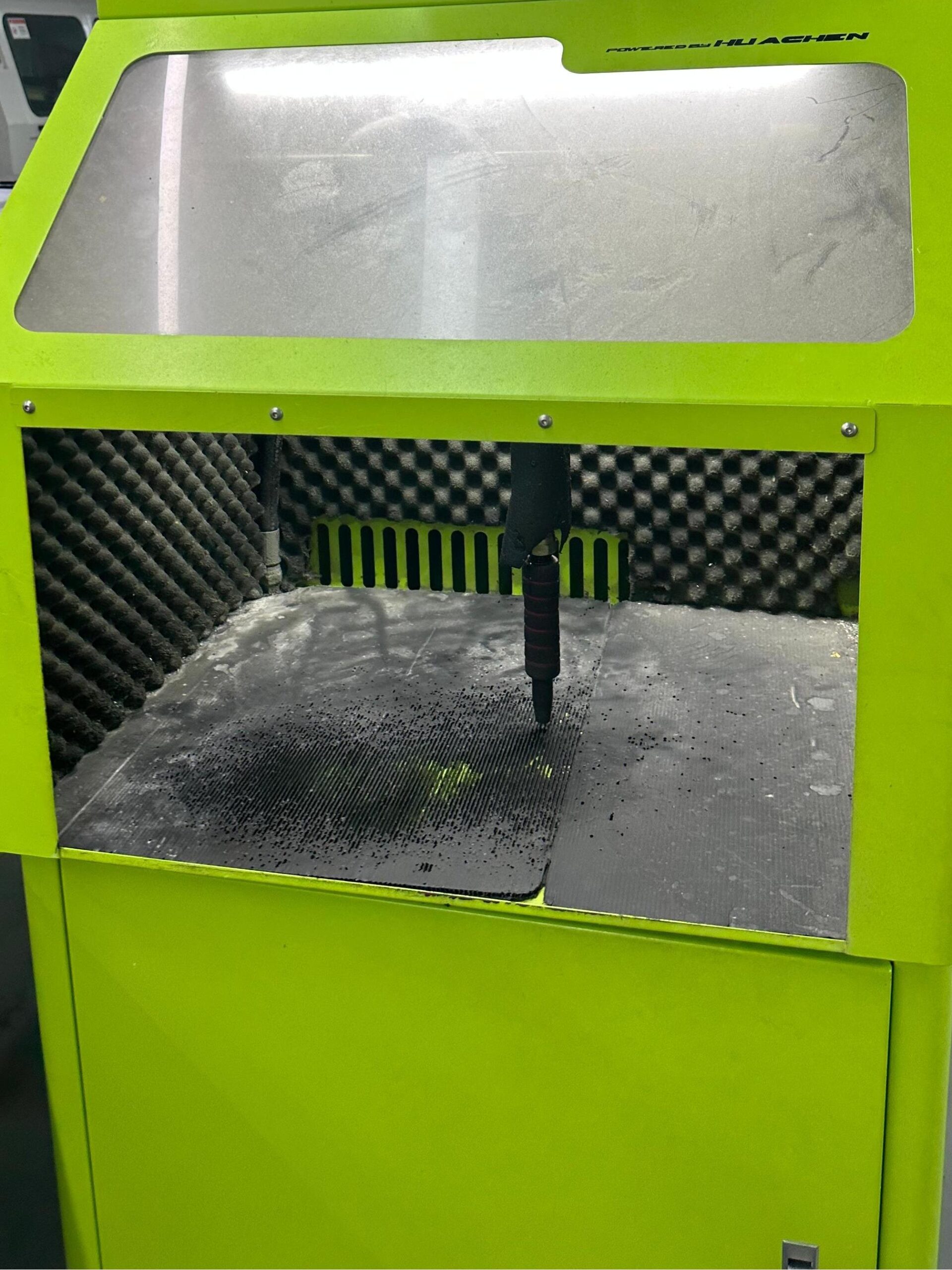
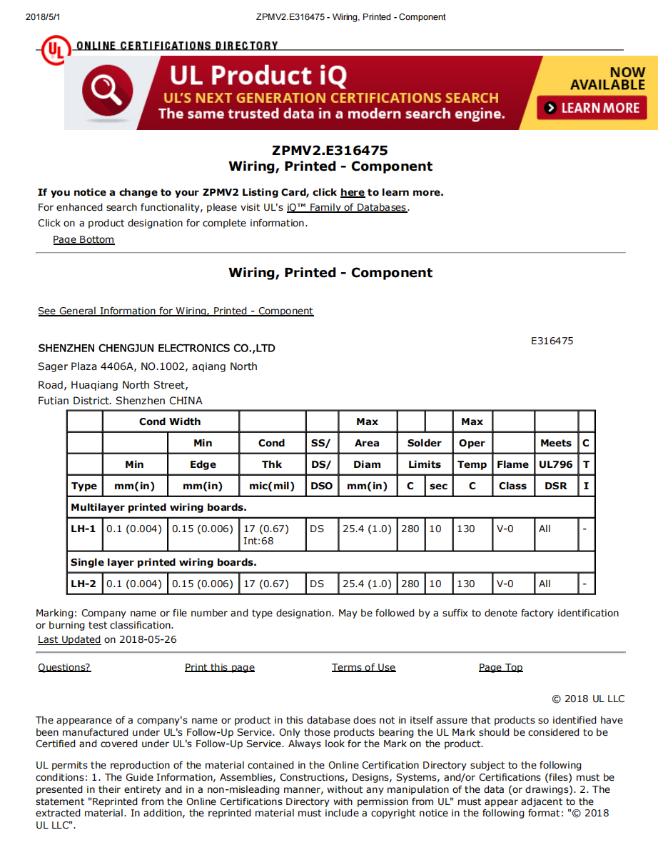
PCB Manufacturing
Uploaded my Gerber files, got a quote in hours, and parts arrived sooner than quoted. Nice.”
PCBA Prototyping& Batch production
I am happy to find you(Jason)!No minimum order hassle, and the soldering looks good, cleanly well.
PCBA and components and modules.
We tested all, PCBs works well, thank you! Michael.
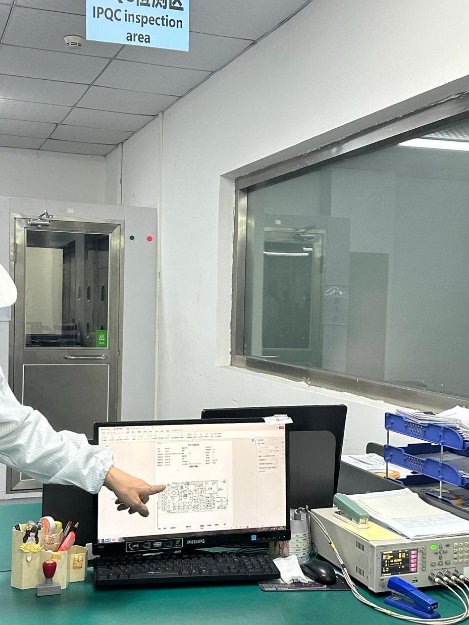
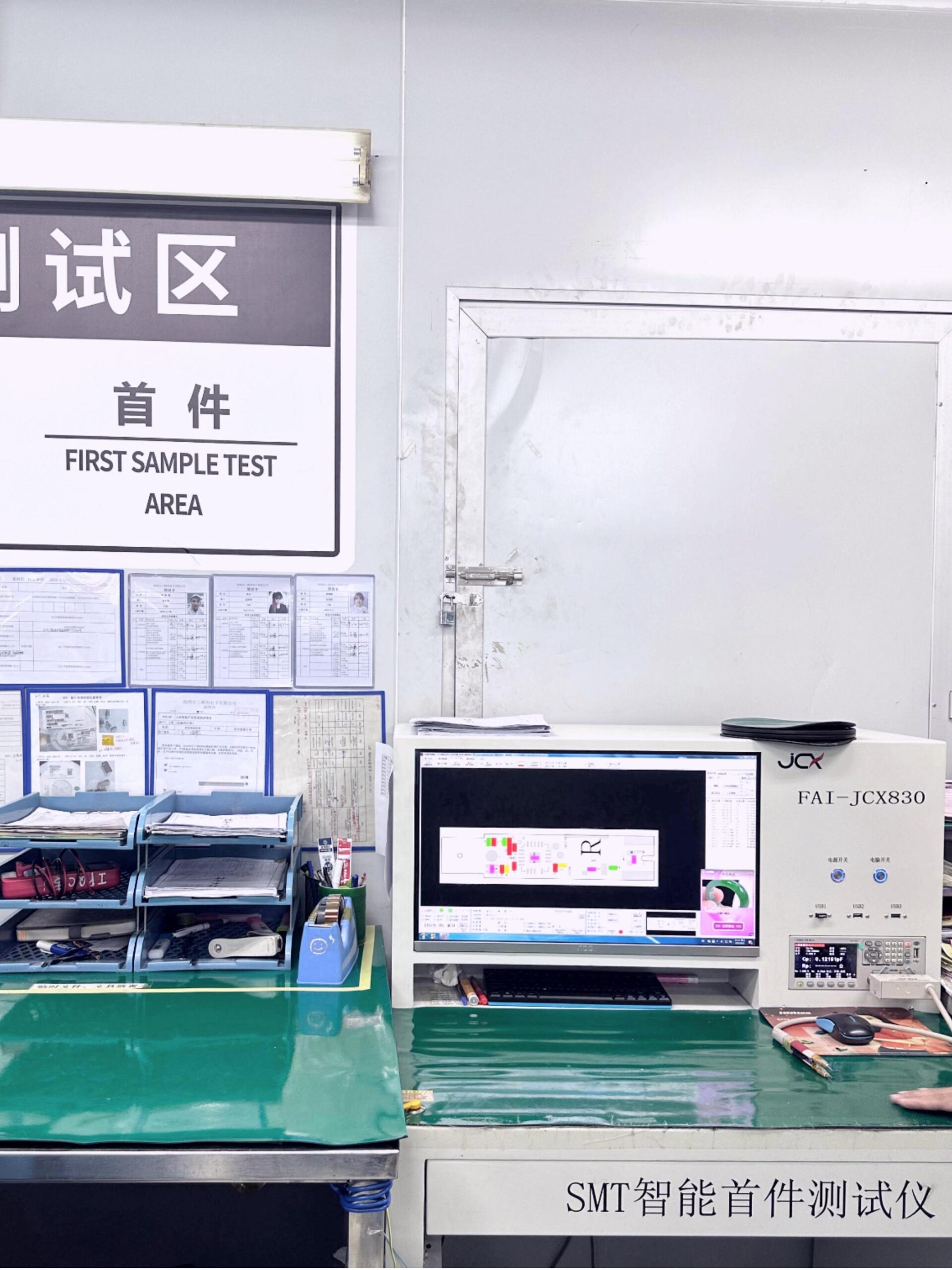
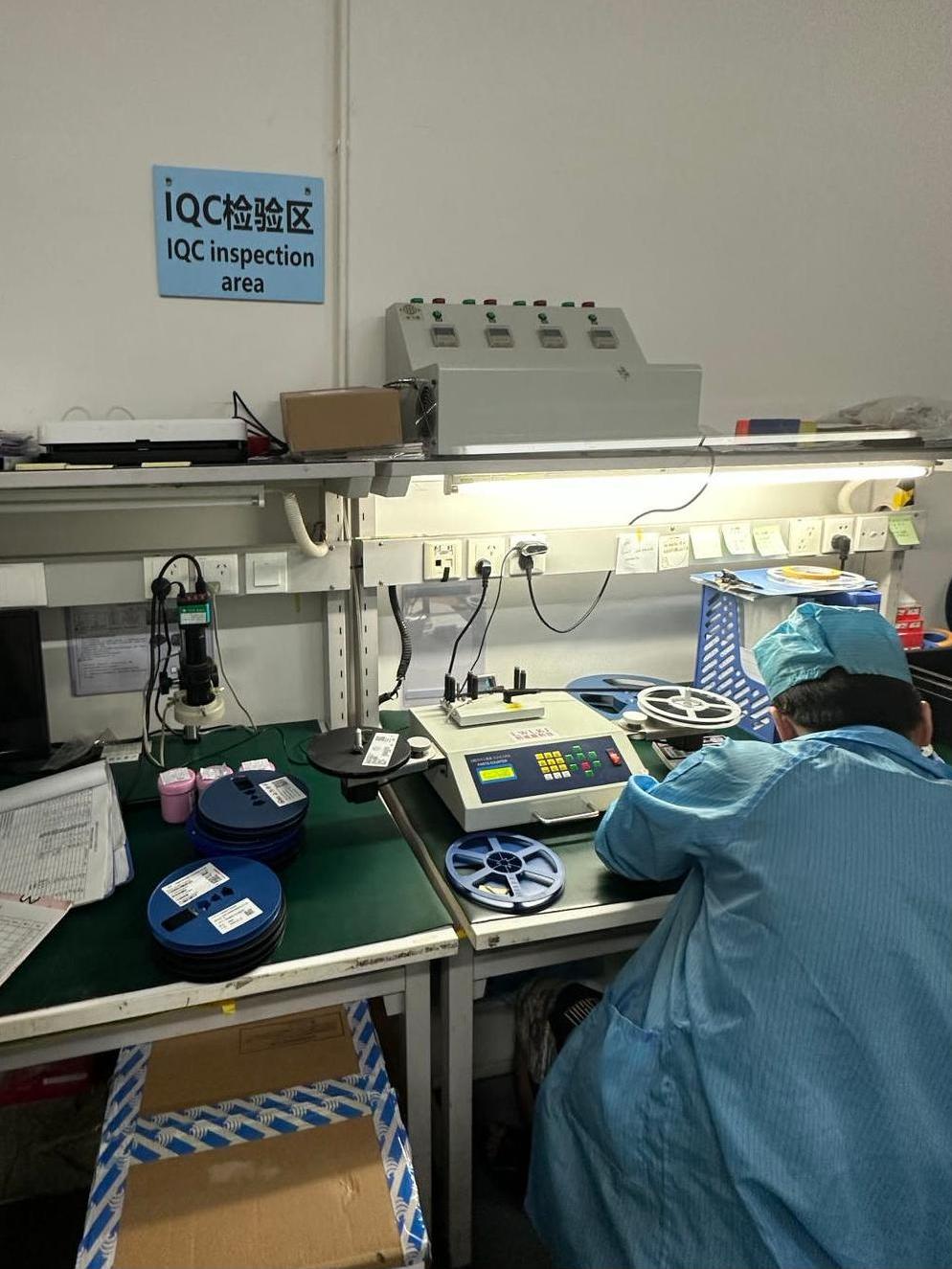
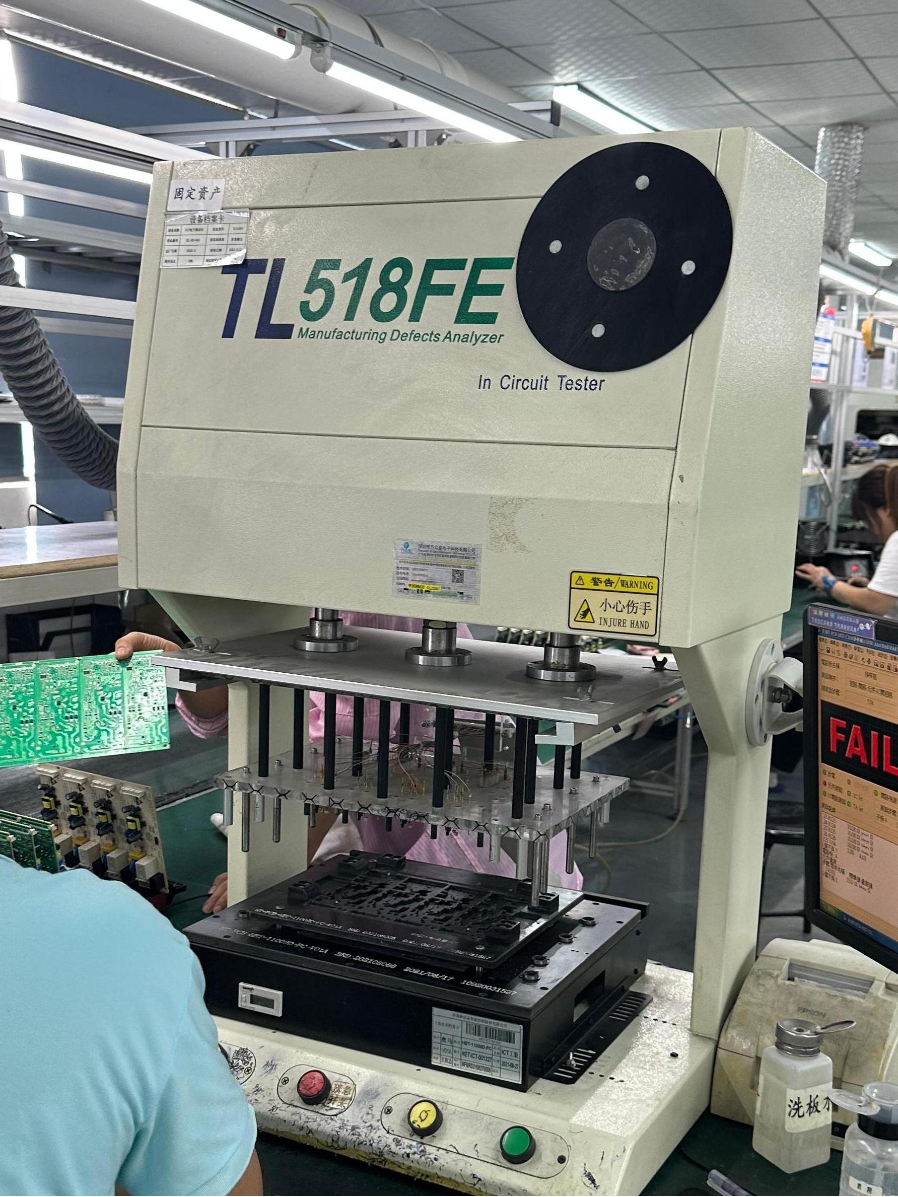
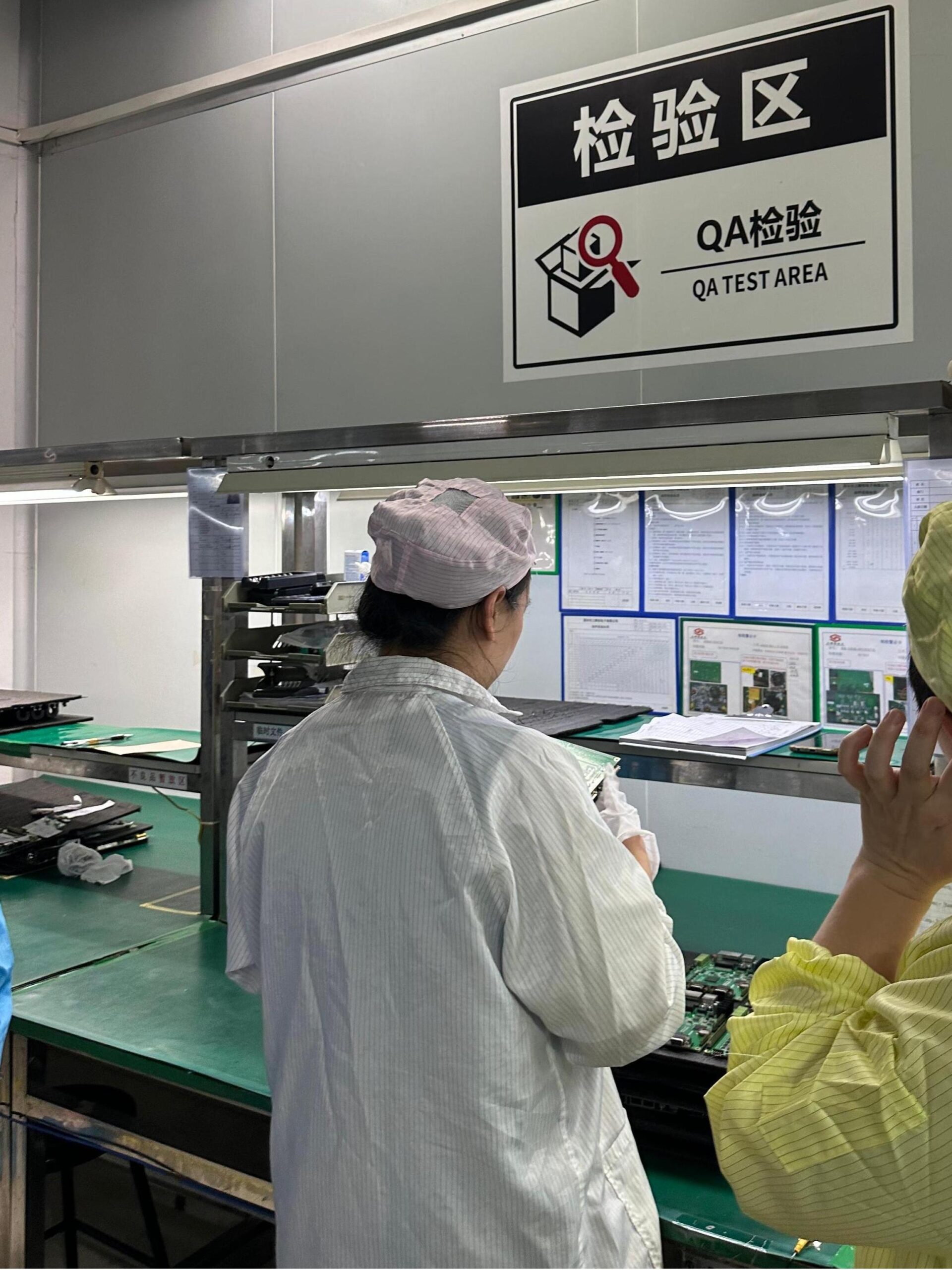
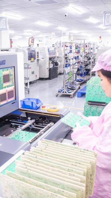
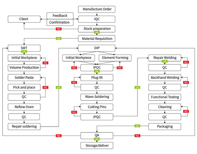
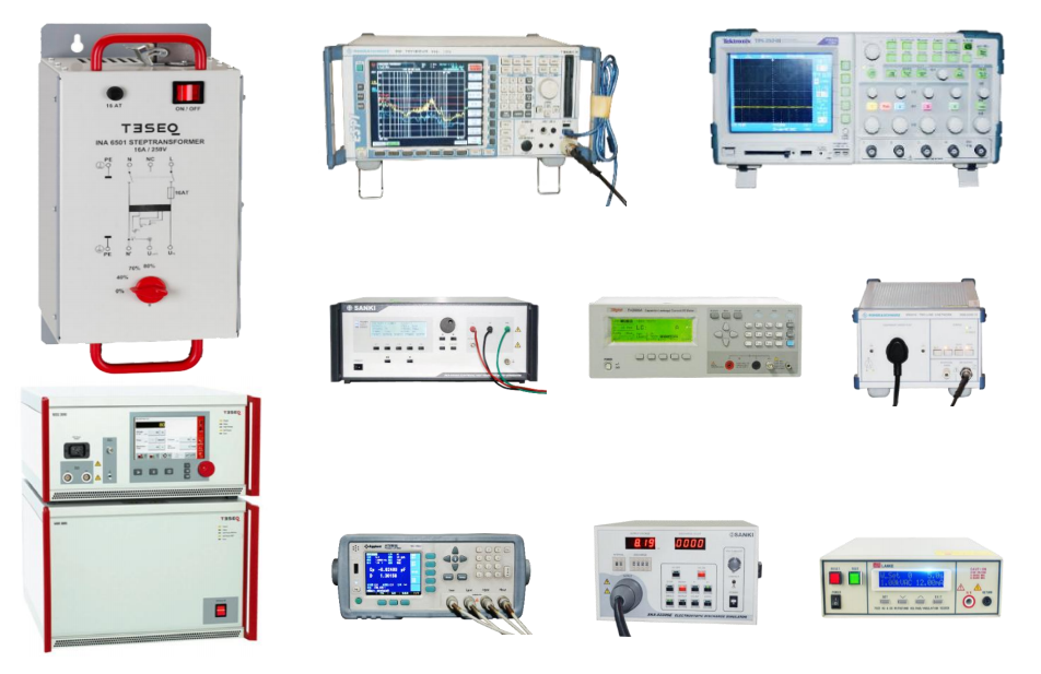
PCB Assembly&Testing
Consistently excellent. Quick responses from Joy.